
Motivation
Remember that only limited researchers have access to high-end micro-/nanofabrication facilitates worldwide. Processes and materials we are currently relying on may not be the best out of available options. We look for better processes for conventional micro-/nanofabrication materials and better materials to realize high-performance transducers.
Research Interests
Large scale batch fabrication of nanostructures based on silicon self-assembly, Hydrogel based micro-/nanoelectromechanical systems, Materials and processing for flexible, stretchable, and wearable devices, Nanoscale 3D printing of organic and inorganic hybrids, 3D printing for biomedical applications, Multifunctional atomic force microscopy, Single molecule force/mass spectroscopy, High-precision Laser based manufacturing and metrology, Additive manufacturing, Heat transfer.
Current ongoing research topics
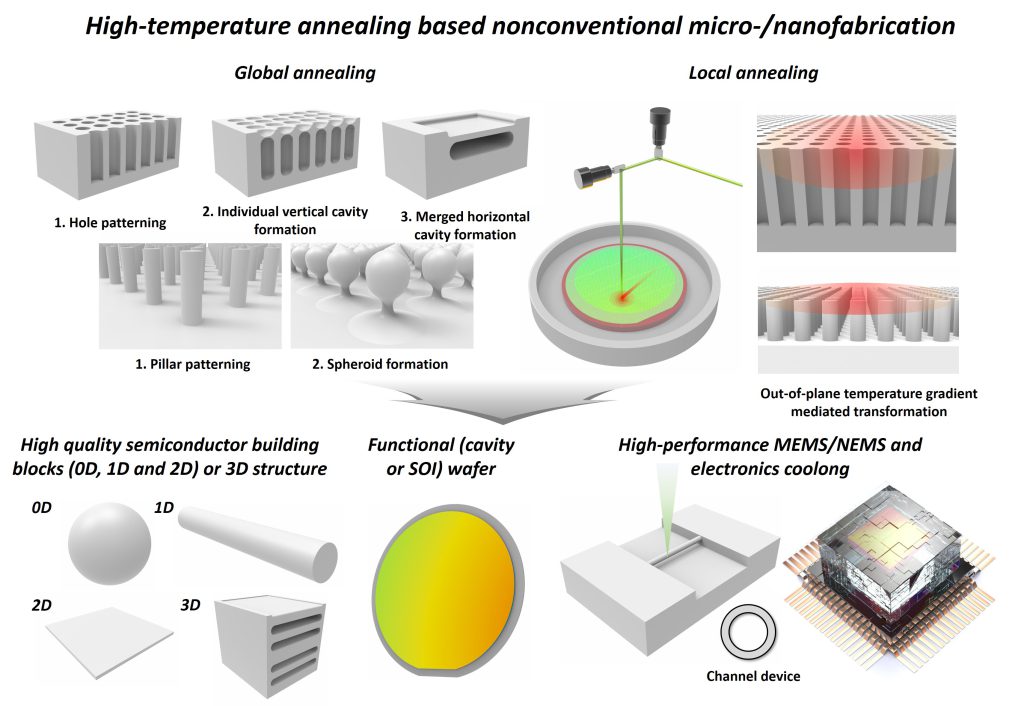
1. Manufacturing & Fabrication
-
In integrated circuits (IC) and micro/nano-electromechanical systems (MEMS/NEMS), annealing is a common technique used to relieve stress in semiconductor materials, redistribute or activate dopants, heal implantation damage, and promote interfacial reactions at metal contacts. It is noteworthy that annealing can induce shape evolution or transformation in pre-structured semiconductor materials, thereby minimizing surface energy. This phenomenon enables the fabrication of distinctive semiconductor micro/nano structures through a combination of standard etching and annealing procedures. The resulting products, formed by annealing semiconductor materials at high temperatures, encompass a range of structures, including membrane-cavity and pedestal spherical structures. The aforementioned structures serve as the basis for the fabrication of high-quality semiconductor materials, functional wafers, and high-performance micro/nano devices.
2. Sensing & Instrumentation
Hyper-multimodal measurements
with heater-integrated microchannel resonator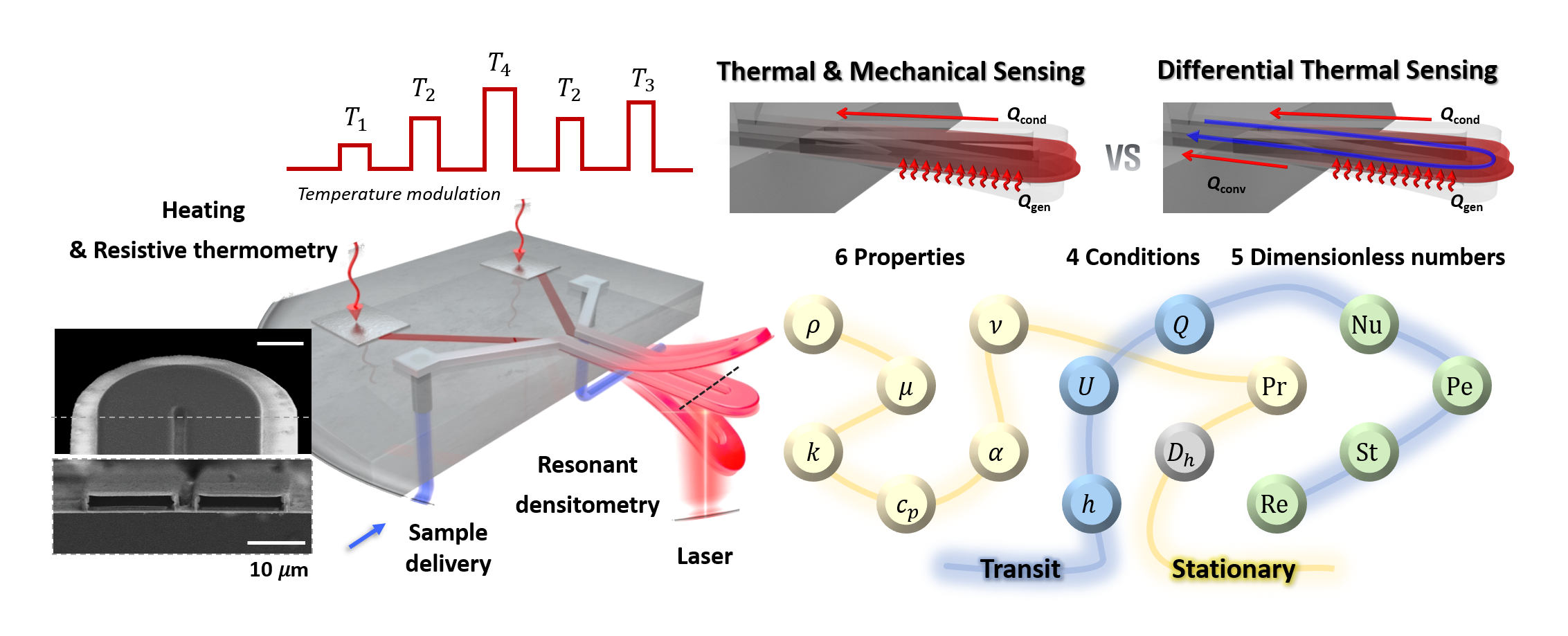
-
Heater-integrated microchannel resonator (HMR) is a system that integrates its key components for the first time, enabling simultaneous resonant densitometry, viscometry, and resistive thermometry. It operates in two distinct modes based on the state of the fluid sample: a stationary mode, where the liquid remains static without flow, and a transit mode, where the liquid flows through the device. 1) In the stationary mode, pressure at the channel inlet and outlet is balanced to keep the liquid static. This mode leverages the dependence of temperature response and mechanical behavior during controlled pulsed heating on the thermophysical and mechanical properties of the liquid inside the channel. By measuring temperature and mechanical resonance changes over time at high power levels, thermophysical properties, including thermal conductivity (k) and specific heat capacity (cp), and mechanical properties, such as density (ρ) and dynamic viscosity (μ), are determined. Furthermore, combined properties like thermal diffusivity (α) and kinematic viscosity (ν), along with dimensionless parameter such as the Prandtl number (Pr), is derived. 2) In the transit mode, consistent liquid flow is maintained by controlling the pressure at the inlet and outlet. The temperature is kept constant using a feedback loop (PID control) by adjusting the heating power input (Q). This mode enables the measurement of average flow velocity (U) and convective heat transfer coefficient (h). Nusselt (Nu) number is derived from this mode, and other dimensionless parameters such as Peclet (Pe), Stanton (St), and Reynolds (Re) numbers are expressed by the integration of information from two operating modes. 3) Collectively, stationary and transit modes enable the HMRs to perform hyper-multimodal measurements, including six thermal and physical properties, four flow and device conditions, and five dimensionless numbers across various temperature levels.
Functionalized microchannel resonator for selective measurement of specific ionic targets
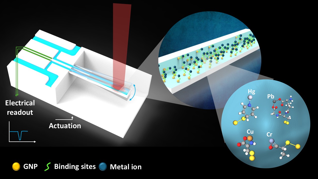
- The functionalized Suspended Microchannel Resonator (SMR) is a mass-based sensing platform designed for sensitive and selective detection of toxic heavy metal ions, including Hg²⁺, Pb²⁺, Cu²⁺, and Cr³⁺, in aqueous environments. This system integrates silicon microfabrication, nanoparticle-based functionalization, and precision resonance measurement into a real-time sensor. The core technology relies on a suspended microchannel resonator fabricated using the Silicon-on-Nothing (SON) technique. Its hollow structure allows fluid to pass through while maintaining mechanical resonance, which shifts in frequency when target ions bind to the inner channel surface. To enable selectivity, the inner walls of the microchannel are chemically functionalized. Gold nanoparticles are deposited to increase surface area and serve as binding anchors. The channel is then modified with a specific ligand depending on the ion to be detected. These functional layers provide molecular recognition, allowing only the target ion to bind effectively. Upon exposure to a contaminated sample, the captured ions increase the effective mass of the resonator, resulting in a measurable downshift in its resonance frequency. This frequency shift is detected either optically or electrically, enabling label-free quantification of ion concentration.